Why it matters: Moore’s Law might not be dead after all. A new technique using nanomaterials can further miniaturize transistors, allowing fab plants to pack more of them on each chip. This research opens up new possibilities for creating advanced semiconductor devices with features smaller than current lithography techniques allow.
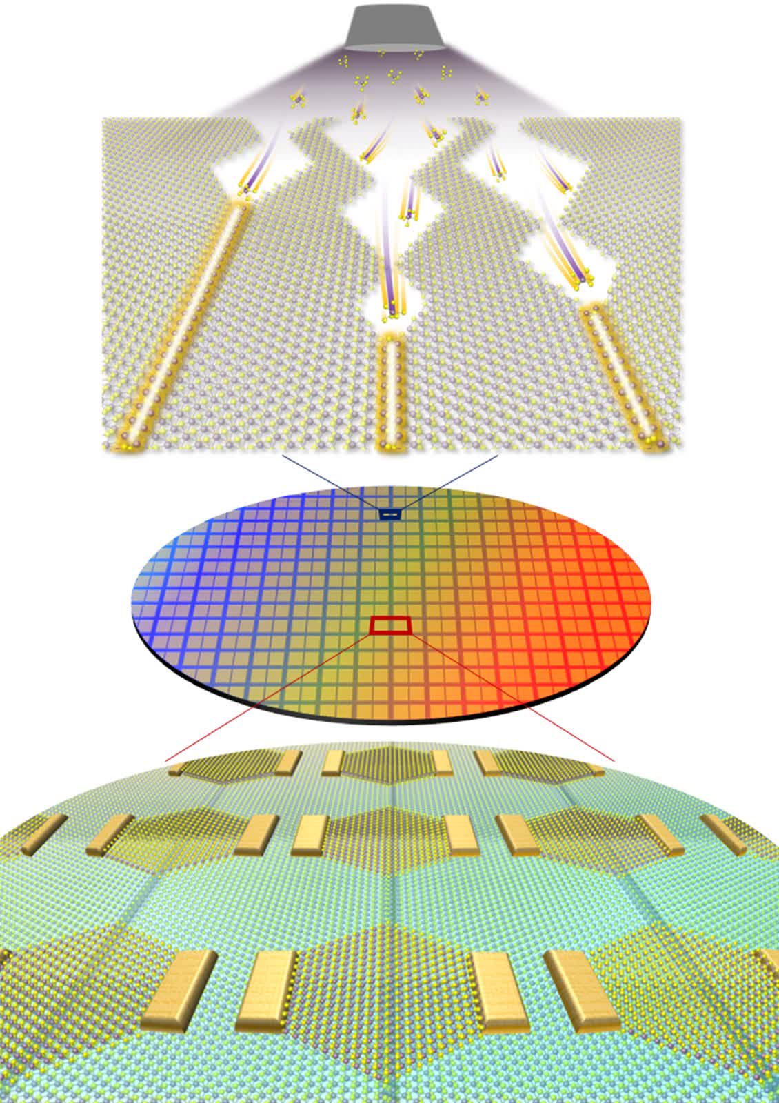
A South Korean research team led by Director Jo Moon-Ho of the Center for Van der Waals Quantum Solids within South Korea’s Institute for Basic Science has made a significant advancement in semiconductor and nanomaterial technology that could lead to the development of much smaller, more efficient, and more powerful electronic devices. The new technique can grow “one-dimentional” metallic nanaomaterials with widths as narrow as 0.4 nanometers for use as gate electrodes on 2D substrates. The technique promises to overcome the limitations of traditional lithography.
Integrated devices based on two-dimensional semiconductors exhibit excellent electrical properties even when thinned to atomic-scale thickness, making them promising candidates for creating ultra-thin, high-performance electronic devices. A separate study indicates that these 2D logic circuits are promising candidates for the post-Moore’s Law era.
However, developing manufacturing processes for integrated circuits based on 2D designs has faced significant hurdles. Integrating 2D materials into devices without damaging their delicate structure is extremely difficult, and achieving consistent large-scale production of high-quality 2D materials is also highly challenging.

Another problem is that current lithography and fabrication techniques don’t work at such small scales. In conventional semiconductor fabrication processes, reducing the gate length below a few nanometers is impossible due to the limitations of lithography resolution.
It is important to note that the degree of integration in semiconductor devices is determined by the width and control efficiency of the gate electrode, which controls the flow of electrons in the transistor. The team leveraged the fact that the mirror twin boundary of molybdenum disulfide, a 2D semiconductor, is a 1D metal with a width of only 0.4 nm. They used this as a gate electrode, overcoming the limitations of the lithography process.
The team could transform the existing 2D semiconductor into a 1D MTB by controlling the crystal structure at the atomic level. These 1D metallic structures can serve as gate electrodes in ultra-miniaturized transistors.
“The 1D metallic phase achieved through epitaxial growth is a new material process that can be applied to ultra-miniaturized semiconductor processes,” said Director JO Moon-Ho. “It is expected to become a key technology for developing various low-power, high-performance electronic devices in the future.”

