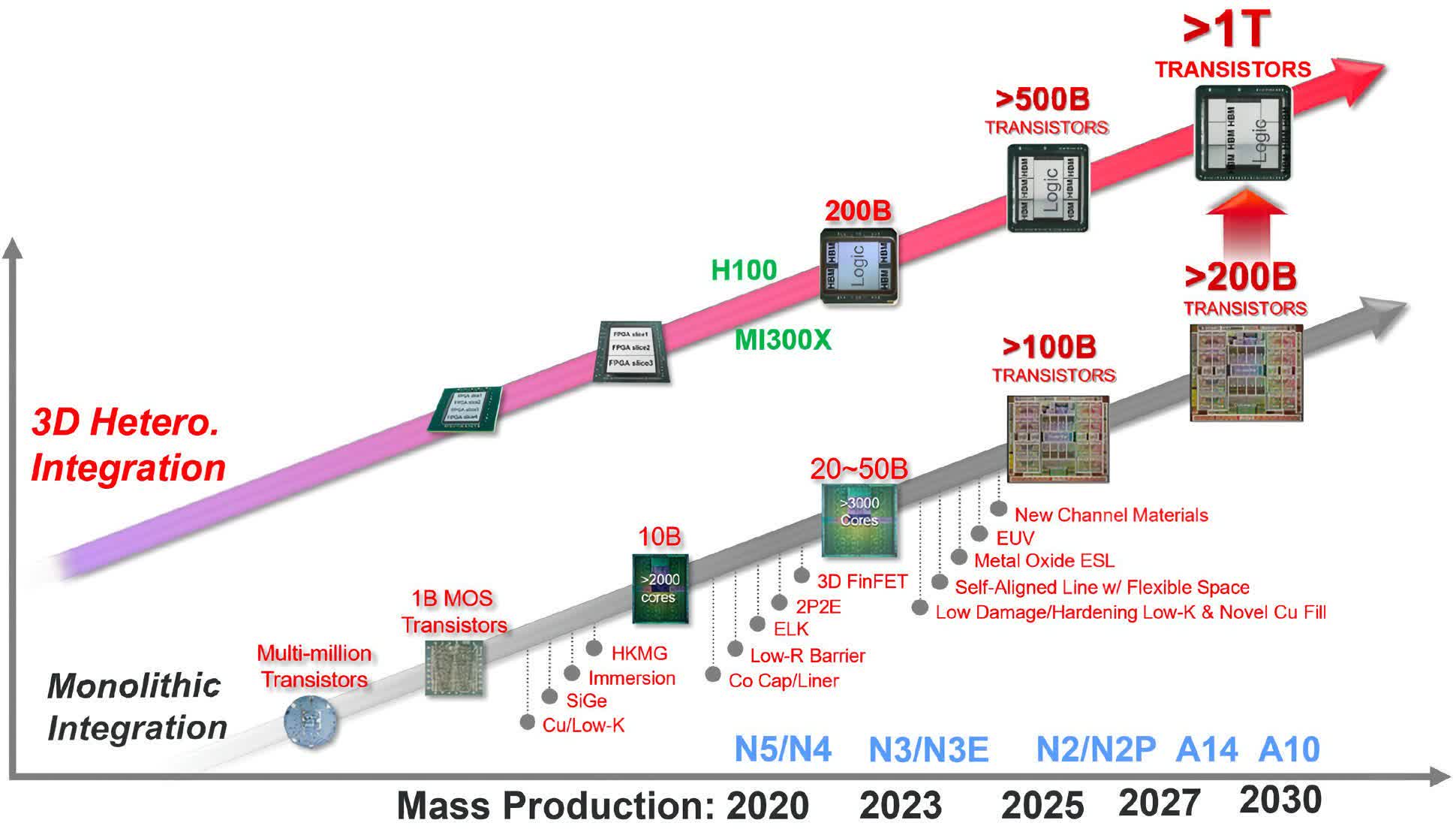
The big picture: The global company showed how it plans to continue increasing transistor density over the next several years. It also believes that the semiconductor industry will transition to chiplet-based designs as well.
At the recent IEDM conference, TSMC unveiled a product roadmap for its semiconductors and next-generation production nodes that culminates in eventually delivering multiple 3D-stacked collections of chiplet designs (3D Hetero Integration) with one trillion transistors on a single chip package. Advancements in packaging technologies, such as CoWoS, InFO and SoIC, will allow it to reach that goal and by 2030 it believes that its monolithic designs could reach 200 billion transistors.
Nvidia’s 80-billion-transistor GH100 is one of the most sophisticated monolithic processors currently on the market. However, as the size of these processors continues to grow and become more costly, TSMC believes that manufacturers will adopt multi-chiplet architectures, such as AMD’s recently-launched Instinct MI300X and Intel’s Ponte Vecchio, which has 100 billion transistors.
For now, TSMC will continue to develop 2nm-class N2 and N2P production nodes and 1.4nm-class A14 and 1nm-class A10 fabrication processes. The company expects to start 2nm production by the end of 2025. In 2028, it will move onto a 1.4nm A14 process, and by 2030, it expects to be producing 1nm transistors.
Meanwhile, Intel is working on its 2nm process (20A), and 1.8nm (18A), which it roughly expects to launch during the same timeframe. One advantage of the new technology is backside power delivery, called PowerVia, which should allow for higher logic densities, higher boost clock speeds, and lower power leakage, resulting in more energy-efficient designs that could outperform TSMC’s offerings.
As the world’s largest foundry, TSMC is confident its process nodes will outperform anything from Intel. In an earnings call, TSMC CEO C.C. Wei said that an internal assessment confirmed the enhancements of the N3P technology and that its 3nm-class manufacturing node demonstrated “comparable PPA” to Intel’s 18A node. He expects N3P to be even better, boasting a more competitive “technology maturity” and having significant cost advantages.
Not one to ignore fighting words, Intel CEO Pat Gelsinger claimed that its 18A process node will outperform TSMC’s 2nm chips despite launching a year earlier.
The market will soon be able to determine which is better. The Taiwan-based chip giant expects to bring N3P into mass production in the second half of 2024 alongside its 20A and 18A products.


